| ITEM | Capability |
| Month Capability | 1000types/month,8,000sqm/month |
| Board Material | Standard FR4: Shengyi, ITEQ, KB, GDM High TG: S1000-2, IT180 |
| Surface treatment | OSP, HASL, LF-HASL, ENIG(Chem. Gold), Immersion Tin, Immersion silver, Plating hard gold, Gold fingers,Flash gold, ENEPIG |
| Tolerance | Board thickness tolerance 1.0mm: +/-0.1mm 1.0mm-2.0mm: +/-10% >2.0mm: +/-8% |
| Hole diameter tolerance PTH: +/-0.075mm NPTH:+/-0.05mm | |
| Hole location tolerance: +/-0.075mm | |
| Outline tolerance: < 100mm: +/-0.1mm 100mm-300mm: +/-0.15mm >300mm: +/-0.2mm | |
| Technical Specification | Layers: 1-24 layers |
| Min line width/space: 0.075/0.075mm | |
| Min hole: 0.15mm (mechanical drilling) 0.1mm (laser drilling) | |
| Min pad ring: 0.1mm | |
| Max copper thickness: 12oz | |
| Max board size:1-2 layers: 635 X 1100mm Multilayers: 500 X 1100mm | |
| Board thickness: 2-layers: 0.2-7.0mm Multi-layers: 0.4-7.0mm Inner layers: 0.1mm | |
| Board warpage: ≤1° | |
| Min solder mask bridge: 0.08mm | |
| Aspect Ration: 8:1 | |
| Plugging Vias capability: 0.2-0.8mm | |
| Au, Ni thickness control: 1. Chem gold: Au:1-10u” 2. Gold fingers: Au:1-150u” 3. Flash gold: Au:1-10u” 4. Hard gold:Au:1-150u” 5. Ni thickness:50-1000u” 6. ENEPIG: Au:1-8u”,Pd:2-5u |

Auto Cutting Machine

Drilling Machine

CNC Routing Machine

Pressing

X-ray Machine

Plating Line

Etching Line

AOI Scanning

AOI Inspection

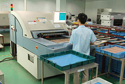
Silkscreen

Dust-free Room

Auto Film Exposure

Auto Gold Immersion Line

Waste Handling 1

Waste Handling 2
")
E-test(E-fixture Test)

Flying Probe Test
")
Flying Probe Test(High Speed)
What is a Printed Circuit Board2014-08-25
A printed circuit board (PCB) mechanically supports and electrically connects electronic components using conductive tracks, pads and other features etched from copper sheets laminated onto a non-condu...
How to Design a Printed Circuit Board2014-08-25
Printed circuit board artwork generation was initially a fully manual process done on clear mylar sheets at a scale of usually 2 or 4 times the desired size. The schematic diagram was first converted i...
Engineering Process before Manufacturing2014-08-25
PCB CAM Manufacturers never use the Gerber or Excellon files directly on their equipment, but always read them into their CAM system. PCBs cannot be manufactured professionally without CAM system. The ...
Patterning of Printed Circuit Board2014-08-25
In subtractive methods the unwanted copper is removed to leave only the desired copper pattern. In additive methods the pattern is electroplated onto a bare substrate using a complex process. The advan...
Chemical Etching2014-08-25
Chemical etching is usually done with ammonium persulfate or ferric chloride. For PTH (plated-through holes), additional steps of electroless deposition are done after the holes are drilled, then coppe...
Inner Layer Manufacturing2014-08-25
Inner layers are used inside multilayer PCBs. Later the inner layers are hardly recognizable from the outside of the finished PCB multi-layer. Inner Layer Automated Optical Inspection (AOI) The inner l...
Drilling Process of Printed Circuit Board2014-08-25
Holes through a PCB are typically drilled with small-diameter drill bits made of solid coated tungsten carbide. Coated tungsten carbide is recommended since many board materials are very abrasive and d...
Solder Resist Application of PCB2014-08-25
Areas that should not be soldered may be covered with solder resist (solder mask). One of the most common solder resists used today is called LPI (liquid photoimageable). A photo sensitive coating is a...
Exposed Conductor Plating and Coating2014-08-25
PCBs are plated with solder, tin, or gold over nickel as a resist for etching away the unneeded underlying copper. After PCBs are etched and then rinsed with water, the solder mask is applied, and then...
Legend Printing of PCB2014-08-25
A legend is often printed on one or both sides of the PCB. It contains the component designators, switch settings, test points and other indications helpful in assembling, testing and servicing the cir...